



HMC7044 Replacement: GX7044 Pin-to-Pin 3.2 GHz Jitter Attenuator
GX7044 is a high-performance clock generator and jitter attenuator developed for high-speed data converters, FPGAs, RF transceivers, local oscillators and digital front-end systems.
The device performs reference selection, frequency conversion, jitter attenuation and low-phase-noise clock distribution. Fourteen configurable outputs support LVPECL, LVDS, CML and LVCMOS signaling standards.
GX7044 uses a 10 mm × 10 mm QFN-68 package designed for pin-to-pin hardware replacement of HMC7044. It supports standard 3.3 V systems and extends the specified operating-temperature range to −55°C to +125°C.
GX7044 as a Pin-to-Pin HMC7044 Replacement
GX7044 integrates two PLL loops for reference conditioning and high-frequency clock generation. PLL2 supports both integer-N operation and a 24-bit fractional-N mode, providing additional flexibility when the required output frequency cannot be generated using integer division alone.
The device provides 14 configurable low-noise outputs with maximum clock frequencies up to 3.2 GHz. The outputs can distribute device clocks and system-reference signals to ADCs, DACs, FPGAs, RF transceivers, local oscillators and DFE ASICs.
For existing HMC7044-based hardware, the GX7044 QFN-68 package provides a pin-compatible migration path. It can also be used in new JESD204B clock-generation and multichannel clock-distribution designs.
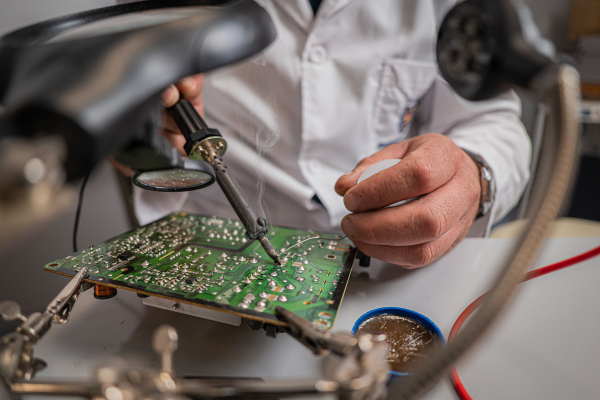
Pin-Compatible QFN-68 Hardware and SPI Control
GX7044 is supplied in a 68-pin QFN package measuring 10 mm × 10 mm and is designed around the HMC7044 package and pin configuration.
The device uses an SPI interface for clock-tree configuration and control. Its output channels support LVPECL, LVDS, CML and LVCMOS modes, allowing the clock outputs to connect to different components within the same RF or data-converter system.
GX7044 operates from 3.15 V to 3.45 V. Existing HMC7044 systems using a 3.3 V supply within this range can retain the original QFN-68 PCB footprint and signal routing.
GX7044 vs HMC7044: Key Specification Comparison
|
Specification |
HMC7044 |
GX7044 |
|
Clock Architecture |
Dual-Loop PLL |
Dual-Loop PLL |
|
PLL Operating Mode |
Integer-N |
Integer-N / 24-Bit Fractional-N |
|
Configurable Outputs |
14 |
14 |
|
Maximum Output Frequency |
3.2 GHz |
3.2 GHz |
|
Output Standards |
LVPECL / LVDS / CML / LVCMOS |
LVPECL / LVDS / CML / LVCMOS |
|
DCLK and SYSREF Generation |
Supported |
Up to Seven DCLK/SYSREF Pairs |
|
JESD204 Support |
JESD204B / JESD204C |
JESD204B |
|
RMS Jitter at 2457.6 MHz |
44 fs Typical, 12 kHz to 20 MHz |
48 fs, 12 kHz to 20 MHz |
|
Noise Floor at 2457.6 MHz |
−156 dBc/Hz |
−153 dBc/Hz |
|
Analog Fine Delay Step |
25 ps |
30 ps |
|
SPI Interface |
Supported |
Supported |
|
Supply Voltage |
3.135–3.465 V |
3.15–3.45 V |
|
Typical Total Supply Current |
586 mA in Specified Normal-Use Profile |
735 mA |
|
Operating Temperature |
−40°C to +85°C |
−55°C to +125°C |
|
Package |
QFN-68, 10 mm × 10 mm |
QFN-68, 10 mm × 10 mm |
|
Pin-to-Pin Compatible |
— |
Yes |
Total supply current depends on the number of enabled channels, selected output standards, divider settings and output operating modes.
GX7044 retains the principal output count, maximum clock frequency, output standards, dual-loop architecture and QFN-68 footprint required by HMC7044-based clock systems. It also provides 24-bit fractional-N operation and a substantially wider specified operating-temperature range.
Clock Generation and Synchronization Features
Key GX7044 features include:
l High-performance dual-loop PLL jitter attenuator
l Integer-N and 24-bit fractional-N operation in PLL2
l Fourteen configurable low-noise clock outputs
l Maximum clock output frequency of 3.2 GHz
l 48 fs RMS jitter from 12 kHz to 20 MHz at 2457.6 MHz
l −153 dBc/Hz noise floor at 2457.6 MHz
l LVPECL, LVDS, CML and LVCMOS output modes
l Up to seven pairs of DCLK and SYSREF signals
l JESD204B clock and synchronization support
l Single-ended and differential output configurations
l 30 ps analog fine-delay step
l SPI configuration interface
l Excellent output crosstalk and frequency isolation
l 3.15 V to 3.45 V supply range
l −55°C to +125°C operating-temperature range
l 10 mm × 10 mm QFN-68 package
GX7044 Applications
GX7044 is suitable for:
l JESD204B clock generation and synchronization
l High-speed ADC and DAC clocking
l Wireless infrastructure equipment
l Multicarrier GSM, LTE and W-CDMA systems
l RF transceiver clock distribution
l Microwave baseband cards
l Phased-array reference distribution
l FPGA and DFE ASIC clocking
l Wide-temperature communication and measurement equipment
Request the GX7044 Datasheet, Samples and Technical Support
GXSC can provide the GX7044 datasheet, QFN-68 pinout information, samples, quotation and technical support for HMC7044 replacement projects and new low-jitter clock-generation designs.
Contact GXSC with your HMC7044 ordering code, reference frequency, required output frequencies, output standards, SYSREF requirements and operating-temperature range to obtain product-selection and replacement support.

 mail
mail