


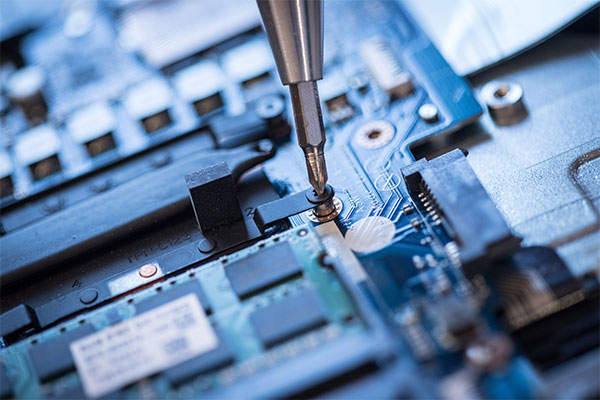
A Comprehensive Guide to the Production Process of Semiconductor Wafers: From Raw Materials to Shipment
Time:2026-05-14
Views:0
The wafer regeneration process refers to a series of procedures that reprocess used silicon wafers to bring them up to standards for reuse. As the foundational material for semiconductor chip manufacturing, wafers undergo multiple high-precision processing steps from the time raw materials are received until the finished products are shipped. The regeneration process primarily includes wafer cleaning, chemical etching, surface polishing, particle removal, and quality inspection to restore the wafer’s surface condition and meet requirements for subsequent use.
The wafer regeneration process places high demands on equipment precision, process control, and quality management to ensure that the wafer’s surface condition, flatness, and cleanliness meet standards for reuse. Taking GXSC’s 6-inch, 8-inch, and 12-inch recycled wafers as examples, the main processing steps are as follows:
1. Wafer Inspection: The initial inspection phase involves visual inspection, thickness measurement, and warpage testing upon receipt of the wafers. Using high-precision equipment, non-conforming wafers with dimensional deviations or abnormal deformation are screened out in advance to prevent defective products from entering subsequent processes.
2. Surface Etching: Through a chemical etching process, residual metal layers, oxide layers, and other coatings on the wafer’s surface and interior are removed. This also eliminates damaged surface layers and processing residues, providing a cleaner, flatter wafer surface for subsequent polishing.
3. Precision Polishing: Wafer polishing requires specialized equipment to perform fine polishing on the wafer surface, enhancing surface flatness and reducing surface roughness while removing surface scratches and some processing-induced damage layers. During polishing, the wafer is also thinned appropriately to achieve a mirror-like smooth finish on one or both sides.
4. Primary Cleaning: The polished wafers are cleaned using specialized equipment to remove contaminants and particles, resulting in finished wafers with pristine surfaces. 5. Final Inspection: After cleaning, the wafers undergo a comprehensive final inspection, primarily assessing surface integrity, wafer thickness, warpage (Warp)/Total Thickness Variation (TTV)/bow, as well as critical electrical resistance parameters.
6. Secondary Cleaning and Packaging: After passing final inspection, a second precision cleaning is performed, followed by packaging according to customer requirements. The two mainstream packaging methods are FOSB professional wafer boxes and coin roll packaging. Sealed packaging effectively isolates the wafers from air, dust, static electricity, and physical damage. 7. Standardized Storage and Shipping: Packaged wafers are transferred to a dedicated storage area for storage and subsequent shipment.
Conclusion: GXSC is equipped with wafer polishing production lines and possesses mature, stable, and scalable production capabilities. We can flexibly handle various batch and customized orders to meet the procurement needs of different customers. Leveraging our comprehensive technical and supply chain systems, we provide a wide range of wafer products and supporting processing services tailored to customer specifications, delivering stable, reliable, and high-quality wafer solutions to the semiconductor industry.

 mail
mail